Facilities
Clean room
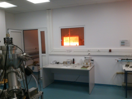
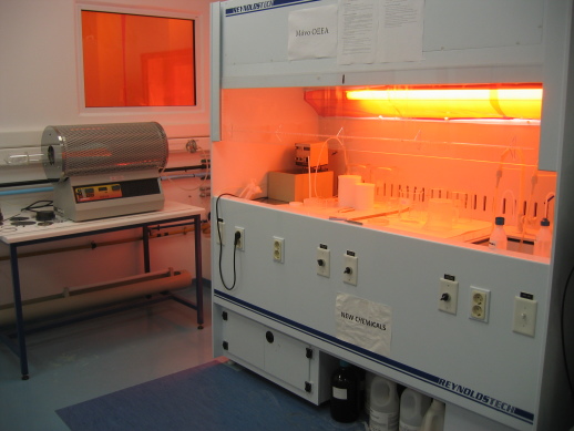
The cleanroom is installed in the Department of Applied Physics of NTUA and it is operational since May 2006. It includes infrastructure for gas distribution, compressed air and vacuum as well as for the provision of de-ionized water with resistivity up to 15 MΩ. Samples are cleaned and dried under class 100 hood areas.
Photos
Vacuum deposition chamber
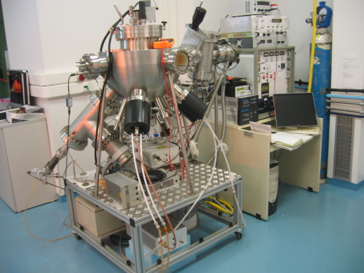
A high vacuum chamber is installed in our clean room and it is equipped with three RF sputtering sources and a nanoparticle DC sputtering source.
The RF sources are used for the deposition of thin films either metallic (Ti, Pt, V) or dielectric (TiO2, V2O5, VO2, HfO2 etc.)
The Nanogen DC nanoparticle source can synthesize and deposit nanoparticles from metallic sources in diameters ranging from 2 to 14 nm and various aerial densities.
Equipment
- 3× Kurt J. Lesker RF Sputtering sources that can operate independently
- 1× Nanogen Magnetron DC Nanoparticle source manufactured by Mantis Deposition Ltd.
- 1× Thermal evaporator for the deposition of Aluminium films
- 1× E-gun evaporator for the deposition of refractory and precious metals with high control of the film thickness
Atomic Layer Deposition
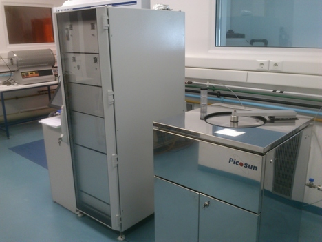
A Picosun R200 Atomic Layer Deposition System is operational since January 2016.
Photos
Inkjet printing station
An inkjet printing solution manufactured by Microdrop Technologies GmbH with a 100 μm nozzle head is also installed in our cleanroom. The printer can deposit polymeric or biological materials with pico-liter resolution.
Electrical characterization laboratory
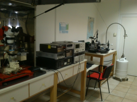
A full range electrical characterization lab is also available. Measurements include Current-Voltage, Capacitance-Voltage, Impedance-Voltage, Pulse sweep, Resistivity, van der Pauw, etc. The available temperature range for the characterization can range from -190°C up to 300°C.
Equipment
- 1× SUSS MicroTec probe station with four probes.
- 2× HP 4140B Picoammeter with two programmable voltage sources
- 1× HP 4096 Impedance analyzer
- 1× Janis Ltd. cryostat (-190°C to 80°C) probe station with two probes.
- 1× Keithley 4200 Parametric Semiconductor analyzer with Pulsed I-V capabilities
- 1× Keithley 2182A Nanovoltmeter with 1× Keithley 7001 switching system for van der Pauw sheet resistance and Hall mobility characterization.
Photos
Laser thermal processing laboratory
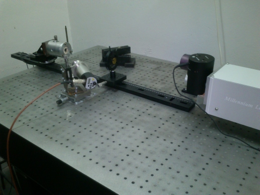
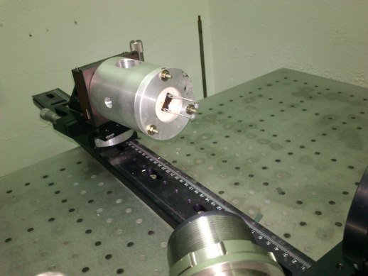
An industrial CO2 laser manufactured by Millenium Lasers Ltd. for the annealing and thermal treatment of semiconductors is installed in our laboratory. The laser can deliver pulses up to 10 kW·cm-2 in the millisecond regime. The setup is also equipped with a heated sample holder (up to 1000°C) to aid the absorption of the radiation in lightly doped semiconductors.
Photos
Nanotechnology characterization laboratory
Our group also operates the nanotechnology characterization center along with the groups of dielectric research, laser research and laser applications
Equipment
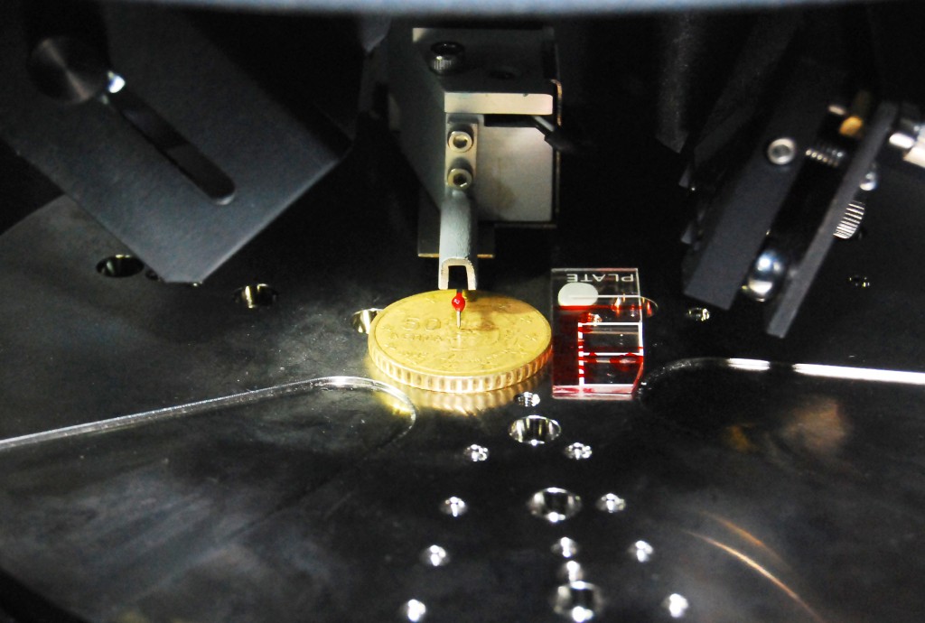
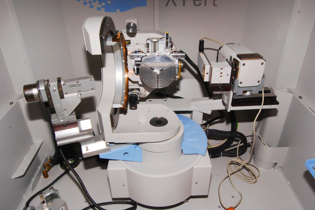
- Panalytical X’Pert X-Ray diffractometer with thin film characterization module
- Dektak 150 stylus profiler
- Veeco diInnova Atomic Force Microscope
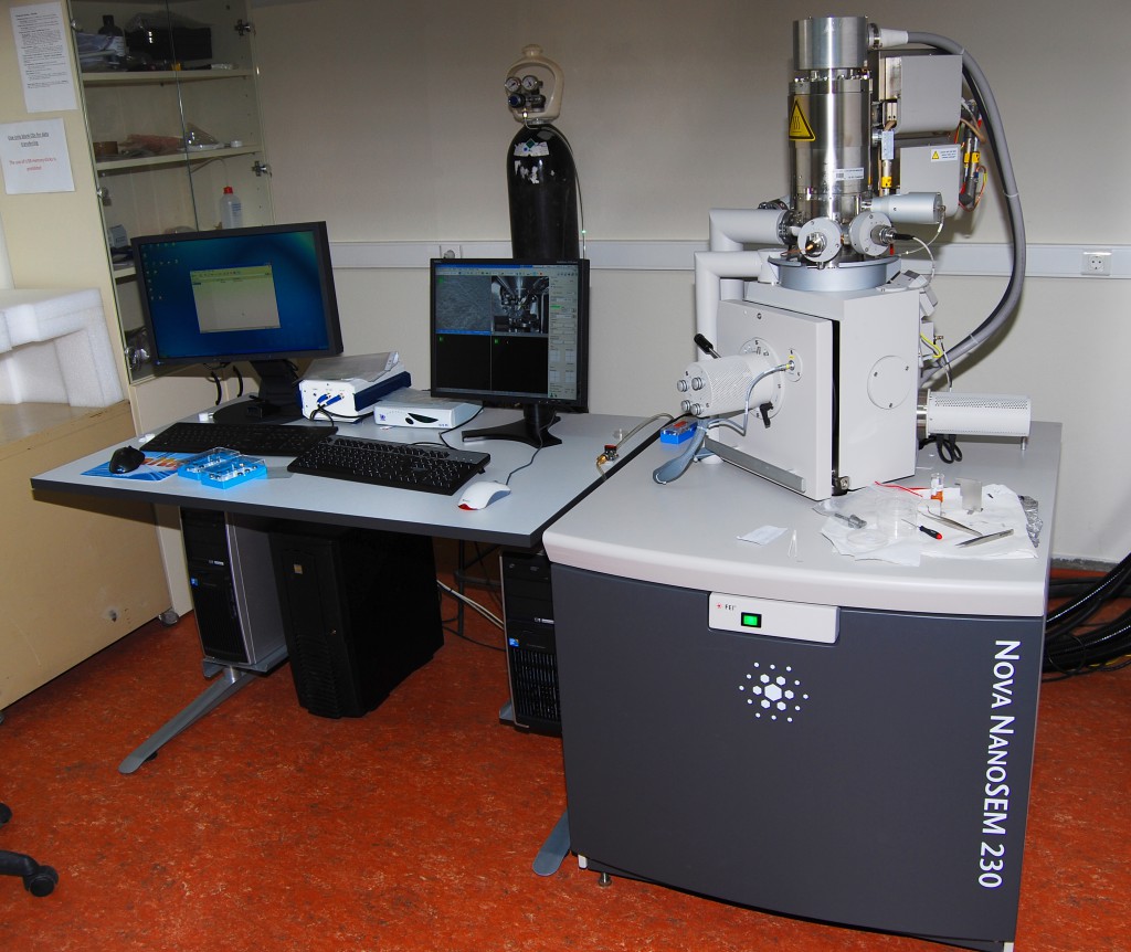
- FEI Nova NanoSEM 230 Scanning Electron Microscope
- Raith Elphy Quantum Electron Beam lithography module for the Nova NanoSEM
Follow this link for more details.
