The main thrust of NANOSOURCE project is the investigation of semiconducting and metallic nanoparticles as active elements of chemical sensors and electronic/optoelectronic devices for charge storage or light emission.
Project Objectives | Project Results
An overall objective of this project is to provide the basis for more permanent collaboration between the academic and industrial partners.
The technical and research objectives are outlined below:
•To develop a process for controlling the size and inter-particle distance of 2-dimensional nanocrystal systems.
•To develop techniques for the formation of 1-D arrays of nanoparticles using electrodynamic self-assembly.
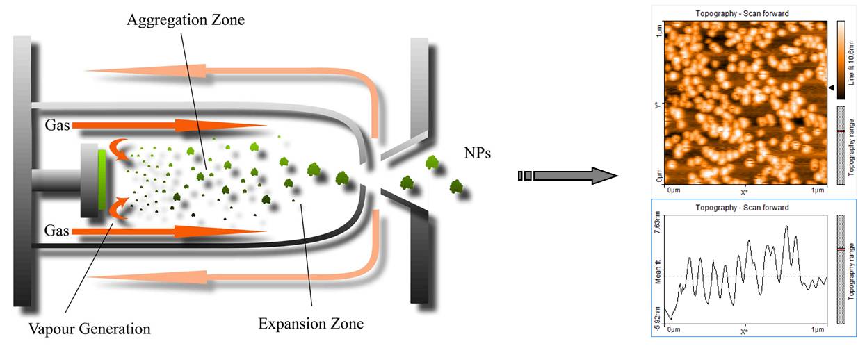
•To characterize the nanoparticle systems to be fabricated by TEM, Scanning Probe Microscopy, Raman spectroscopy, FTIR spectroscopy and Photoluminescence spectroscopy.
•To fabricate and demonstrate application driven devices in the areas of sensors and electronic/optoelectronic devices using the know-how on controlled nanoparticle deposition.
Click here to view the Project Results